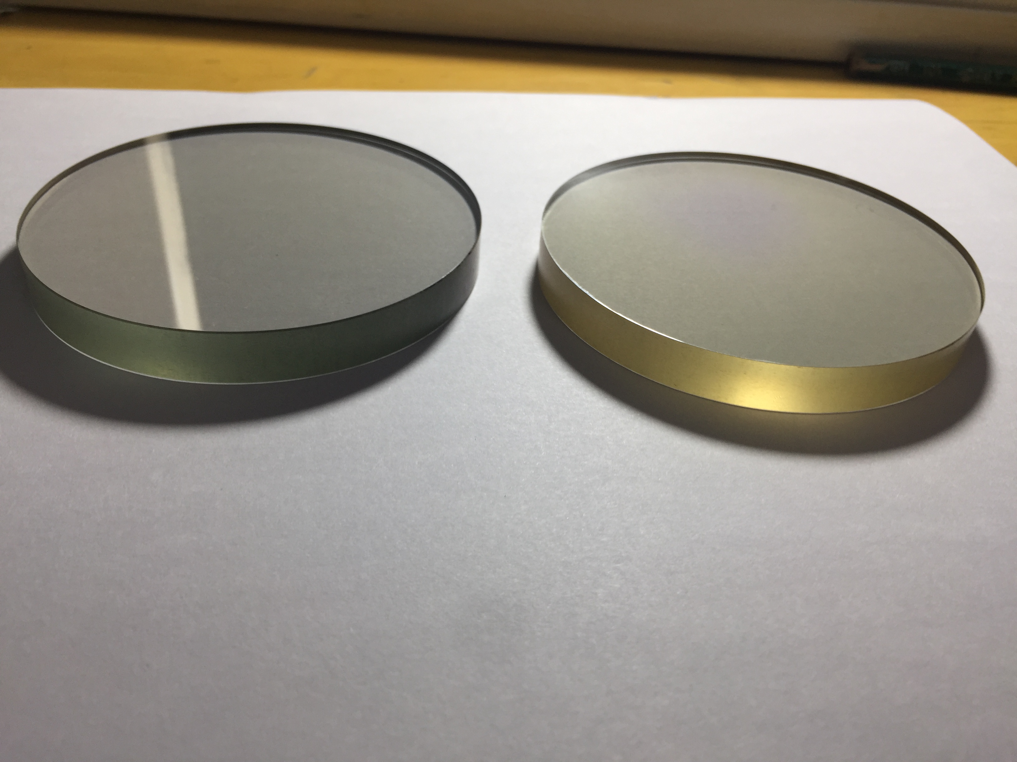
N-type silicon carbide substrate material is an essential material to support the development of the power electronics industry.Its outstanding physical characteristics such as high-pressure resistance and high-frequency resistance can be widely used in high-power high-frequency electronic devices, electric vehicle PCU, photovoltaic inverter, rail transit power control system and other fields, and can play a role of reducing volume simplification system and improving power density.
| Main performance parameters | |||
| Growth method | Seed crystal sublimation method, PVT (Physical gas phase transfer) | ||
| Crystal structure | Hexagon | ||
| Lattice constant | a=3.08 Å ,c=15.08 Å | ||
| Marshalling sequence | ABCACB(6H), ABCBABCB(4H) | ||
| Band gap | 2.93 eV | ||
| Mohs hardness | 9.2 | ||
| Heat conductivity @300K | 5 W/ cm.k | ||
| Dielectric constant | e(11)=e(22)=9.66 e(33)=10.33 | ||
| Conductor type | I | N | |
| Dopant | Undoped | Vanadium | Nitrogen |
| Resistivity (ohm.cm) | ˃ 1*107 | ˃ 1*105 | 0.01-0.2 |
| Dimension | 5x5,10x10,15x15,20x20, | ||
| Ø50.8, Ø100 mm, Ø150mm等 | |||
| Thickness | 0.33/0.35/0.5mm, Special direction and size of the substrate can be customized according to the customer need | ||
| Polishing | One side or two sides | ||
| Orientation | <0001>or <0001> off 4.0º | ||
| Orientation tolerance | ±0.5° | ||
| Flat orientation tolerance | 2°(special requirements 1°) | ||
| Roughness | ≤5Å(5µm×5µm) | ||
| Packing | Class 100 clean bag, Class 1000 clean room | ||